Power supply from a mobile phone charger. How to convert a cell phone charger to a different voltage
Now all cell phone manufacturers have agreed and everything that is in stores is charged via a USB connector. This is very good because chargers have become universal. In principle, a cell phone charger is not such a thing.
This is only a pulsed direct current source with a voltage of 5V, and the charger itself, that is, the circuit that monitors the battery charge and ensures its charge, is located in the cell phone itself. But that’s not the point, the point is that these “chargers” are now sold everywhere and are already so cheap that the issue of repairs somehow disappears by itself.
For example, in a store “charging” costs from 200 rubles, and on the well-known Aliexpress there are offers from 60 rubles (including delivery).
Schematic diagram
A typical Chinese charging circuit, copied from the board, is shown in Fig. 1. There may also be an option with swapping diodes VD1, VD3 and zener diode VD4 to the negative circuit - Fig. 2.
And more “advanced” options may have rectifier bridges at the input and output. There may also be differences in part ratings. By the way, the numbering on the diagrams is given arbitrarily. But this does not change the essence of the matter.
Rice. 1. Typical circuit diagram of a Chinese network charger for a cell phone.
Despite its simplicity, this is still a good switching power supply, and even a stabilized one, which is quite suitable for powering something other than a cell phone charger.

Rice. 2. Circuit diagram of a network charger for a cell phone with a changed position of the diode and zener diode.
The circuit is made on the basis of a high-voltage blocking generator, the width of the generation pulses is regulated using an optocoupler, the LED of which receives voltage from the secondary rectifier. The optocoupler reduces the bias voltage based on the key transistor VT1, which is set by resistors R1 and R2.
The load of transistor VT1 is the primary winding of transformer T1. The secondary, step-down winding is winding 2, from which the output voltage is removed. There is also winding 3, it serves both to create positive feedback for generation, and as a source of negative voltage, which is made on diode VD2 and capacitor C3.
This negative voltage source is needed to reduce the voltage at the base of transistor VT1 when optocoupler U1 opens. The stabilization element that determines the output voltage is the zener diode VD4.
Its stabilization voltage is such that, in combination with the direct voltage of the IR LED of the optocoupler U1, it gives exactly the necessary 5V that is required. As soon as the voltage at C4 exceeds 5V, the zener diode VD4 opens and current flows through it to the optocoupler LED.
And so, the operation of the device does not raise any questions. But what if I need not 5V, but, for example, 9V or even 12V? This question arose along with the desire to organize a network power supply for a multimeter. As you know, multimeters, popular in amateur radio circles, are powered by Krona, a compact 9V battery.
And in “field” conditions this is quite convenient, but in home or laboratory conditions I would like power from the mains. According to the diagram, “charging” from a cell phone is in principle suitable, it has a transformer, and the secondary circuit is not in contact with the electrical network. The only problem is the supply voltage - “charging” produces 5V, but the multimeter needs 9V.
In fact, the problem of increasing the output voltage is solved very simply. You just need to replace the zener diode VD4. To obtain a voltage suitable for powering a multimeter, you need to set the zener diode to a standard voltage of 7.5V or 8.2V. In this case, the output voltage will be, in the first case, about 8.6V, and in the second about 9.3V, which, both of them, are quite suitable for a multimeter. Zener diode, for example, 1N4737 (this is at 7.5V) or 1N4738 (this is at 8.2V).
However, you can use another low-power zener diode for this voltage.
Tests have shown good operation of the multimeter when powered from such a power source. In addition, we tried an old pocket radio powered by a Krona, and it worked, only interference from the power supply was a slight hindrance. The matter is not limited to 9V voltage at all.

Rice. 3. Voltage regulation unit for converting a Chinese charger.
Do you want 12V? - No problem! We set the zener diode to 11V, for example, 1N4741. You just need to replace capacitor C4 with a higher voltage one, at least 16V. You can get even more tension. If you remove the zener diode altogether, there will be a constant voltage of about 20V, but it will not be stabilized.
You can even make a regulated power supply if you replace the zener diode with a regulated zener diode such as the TL431 (Figure 3). The output voltage can be adjusted, in this case, by variable resistor R4.
Karavkin V. RK-2017-05.
Power source - from a cell phone charger
I. NECHAYEV, Kursk
Small-sized portable equipment (radios, cassette and disc players) are usually powered by two to four galvanic cells. However, they do not last long, and they have to be replaced with new ones quite often, so at home it is advisable to power such equipment from a power supply. Such a source (in common parlance it is called an adapter) is not difficult to purchase or make yourself; fortunately, there are many of them described in amateur radio literature. But you can do it differently. Almost three out of every four residents of our country today have a cell phone (according to the research company AC&M-Consulting, at the end of October 2005, the number of cellular subscribers in the Russian Federation exceeded 115 million). Its charger is used for its intended purpose (to charge the phone battery) only a few hours a week, and the rest of the time is inactive. The article describes how to adapt it to power small-sized equipment.
In order not to spend money on galvanic elements, owners of wearable radios, players, etc. equipment use batteries, and in stationary conditions they power these devices from an alternating current network. If you don’t have a ready-made power supply with the required output voltage, you don’t have to buy or assemble such a unit yourself; you can use a cell phone charger for this purpose, which many people have today.
However, you cannot directly connect it to a radio or player. The fact is that most chargers included with a cell phone are an unstabilized rectifier, the output voltage of which (4.5...7 V at a load current of 0.1...O.3A) exceeds that required to power a small-sized apparatus. The problem can be solved simply. To use the charger as a power supply, you must connect a voltage stabilizer adapter between it and the device.
As the name itself says, the basis of such a device should be a voltage stabilizer. It is most convenient to assemble it on a specialized microcircuit. The large range and availability of integrated stabilizers allow us to produce a wide variety of adapter options.
The schematic diagram of the adapter-voltage stabilizer is shown in Fig. 1. DA1 chip is selected 
depending on the required output voltage and current consumed by the load. The capacitance of capacitors C1 and C2 can be in the range of 0.1...10 µF (rated voltage - 10 V).
If the load consumes up to 400 mA and the charger can supply such current, the KR142EN5A (output voltage - 5 V), KR1158ENZV, KR1158ENZG (3.3 V), KR1158EN5V, KR1158EN5G (5 V) microcircuits can be used as DA1, as well as five-volt imported 7805, 78M05. Microcircuits of the LD1117xxx, REG 1117-xx series are also suitable. Their output current is up to 800 mA, the output voltage is from the range 2.85; 3.3 and 5 V (for LD1117xxx - also 1.2; 1.8 and 2.5 V). The seventh element (letter) in the designation LD1117xxx indicates the type of housing (S - SOT-223, D - S0-8, V - TO-220), and the two-digit number following it indicates the nominal value of the output voltage in tenths of volts (12 - 1.2 V, 18 - 1.8 V, etc.). The number attached through a hyphen in the designation of REG1117-xx microcircuits also indicates the stabilization voltage. The pinout of these microcircuits in the SOT-223 package is shown in Fig. 2, a.
It is also acceptable to use stabilizer microcircuits with adjustable output voltage, for example, KR142EN12A, LM317T. In this case, you can get any output voltage value from 1.2 to 5...6 V.
When powering equipment that consumes a small current (30..100 mA), for example, small-sized VHF FM radios, the adapter can use the KR1157EN5A, KR1157EN5B, KR1157EN501A, KR1157EN501B, KR1157EN502A, KR1157EN502B, 8EN5A, KR1158EN5B (all with rated output voltage 5 V ), KR1158ENZA, KR1158ENZB (3.3 V). Drawing of a possible version of the adapter printed circuit board using
The use of microcircuits of the latest series is shown in Fig. 3. Capacitors C1 and C2 - small-sized oxide capacitors of any type with a capacity of 10 μF.
The dimensions of the adapter can be significantly reduced by using miniature microcircuits of the LM3480-xx series (the last two digits indicate the output voltage). They are produced in the SOT-23 package (see Fig. 2.6). The printed circuit board drawing for this case is shown in Fig. 4. Capacitors C1 and C2 - small-sized ceramic K10-17 or similar imported ones with a capacity of at least 0.1 μF. Appearance of adapters mounted on boards manufactured in accordance with Fig. 3 and 4, shown in Fig. 5. 
It should be noted that the foil on the board can serve as a heat sink. Therefore, it is advisable to make the area of the conductor for the microcircuit terminal (common or output), through which heat is removed, as large as possible.
The assembled device is placed in a plastic box of suitable dimensions or in the battery compartment of the powered device. To connect to the charger, the adapter must be equipped with an appropriate socket (similar to the one installed in a cell phone). It can be placed on a printed circuit board with a stabilizer or mounted on one of the walls of the box.
The adapter does not require installation, you just need to check it in operation with the connecting wires that will be used to connect to the charger and the powered device. Self-excitation is eliminated by increasing the capacitance of capacitors C1 and C2.
LITERATURE
1. Biryukov S. Microcircuit voltage stabilizers for wide application. - Radio, 1999, No. 2, p. 69-71.
2. LD1117 Series. Low Drop Fixed and Adjustable Positive Voltage Regulators. -
3. REG1117, REG1117A. 800mA and 1A Low Dropout (LDO) Positive Regulator 1.8V, 2.5V, 2.85V, 3.3V, 5V and Adjustable. -
4. LM3480. 100 mA, SOT-23, Quasi Low-Dropout Linear Voltage Regulator. -
Most modern network chargers are assembled using a simple pulse circuit, using one high-voltage transistor (Fig. 1) according to a blocking generator circuit.
Unlike simpler circuits using a step-down 50 Hz transformer, the transformer for pulse converters of the same power is much smaller in size, which means the size, weight and price of the entire converter are smaller. In addition, pulse converters are safer - if in a conventional converter, when the power elements fail, the load receives a high unstabilized (and sometimes even alternating) voltage from the secondary winding of the transformer, then in case of any malfunction of the “pulse generator” (except for the failure of the reverse optocoupler) connection - but it is usually very well protected) there will be no voltage at the output at all.

Rice. 1
A simple pulse blocking oscillator circuit
A detailed description of the principle of operation (with pictures) and calculation of the circuit elements of a high-voltage pulse converter (transformer, capacitors, etc.) can be read, for example, in “TEA152x Efficient Low Power Voltage supply” at the link http://www. nxp.com/acrobat/applicationnotes/AN00055.pdf (in English).
The alternating mains voltage is rectified by diode VD1 (although sometimes the generous Chinese install as many as four diodes in a bridge circuit), the current pulse when turned on is limited by resistor R1. Here it is advisable to install a resistor with a power of 0.25 W - then if overloaded, it will burn out, acting as a fuse.
The converter is assembled on transistor VT1 according to the classic flyback circuit. Resistor R2 is needed to start generation when power is applied; in this circuit it is optional, but with it the converter works a little more stable. Generation is maintained thanks to capacitor C1, included in the PIC circuit on the winding, the generation frequency depends on its capacitance and the parameters of the transformer. When the transistor is unlocked, the voltage at the lower terminals of windings I and II in the diagram is negative, at the upper terminals it is positive, the positive half-wave through capacitor C1 opens the transistor even more strongly, the voltage amplitude in the windings increases... That is, the transistor opens like an avalanche. After some time, as capacitor C1 charges, the base current begins to decrease, the transistor begins to close, the voltage at the upper terminal of winding II in the circuit begins to decrease, through capacitor C1 the base current decreases even more, and the transistor closes like an avalanche. Resistor R3 is necessary to limit the base current during circuit overloads and surges in the AC network.
At the same time, the amplitude of the self-induction EMF through the diode VD4 recharges the capacitor SZ - that is why the converter is called flyback. If you swap the terminals of winding III and recharge the capacitor SZ during the forward stroke, then the load on the transistor will sharply increase during the forward stroke (it may even burn out due to too much current), and during the reverse stroke the self-induction EMF will be unspent and will be released by collector junction of the transistor - that is, it can burn out from overvoltage. Therefore, when manufacturing the device, it is necessary to strictly observe the phasing of all windings (if you mix up the terminals of winding II, the generator simply will not start, since capacitor C1 will, on the contrary, disrupt generation and stabilize the circuit).
The output voltage of the device depends on the number of turns in windings II and III and on the stabilization voltage of the zener diode VD3. The output voltage is equal to the stabilization voltage only if the number of turns in windings II and III is the same, otherwise it will be different. During the reverse stroke, capacitor C2 is recharged through diode VD2, as soon as it is charged to approximately -5 V, the zener diode will begin to pass current, the negative voltage at the base of transistor VT1 will slightly reduce the amplitude of the pulses on the collector, and the output voltage will stabilize at a certain level. The stabilization accuracy of this circuit is not very high - the output voltage varies within 15...25% depending on the load current and the quality of the zener diode VD3.
A circuit of a better (and more complex) converter is shown in rice. 2

Rice. 2
Electrical circuit of a more complex
converter
To rectify the input voltage, a diode bridge VD1 and a capacitor are used; the resistor must have a power of at least 0.5 W, otherwise at the moment of switching on, when charging capacitor C1, it may burn out. The capacitance of capacitor C1 in microfarads must be equal to the power of the device in watts.
The converter itself is assembled according to the already familiar circuit using transistor VT1. A current sensor on resistor R4 is included in the emitter circuit - as soon as the current flowing through the transistor becomes so large that the voltage drop across the resistor exceeds 1.5 V (with the resistance indicated on the diagram being 75 mA), transistor VT2 opens slightly through diode VD3 and limits the base current of transistor VT1 so that its collector current does not exceed the above 75 mA. Despite its simplicity, this protection circuit is quite effective, and the converter turns out to be almost eternal even with short circuits in the load.
To protect transistor VT1 from emissions of self-induction EMF, a smoothing circuit VD4-C5-R6 was added to the circuit. The VD4 diode must be high-frequency - ideally BYV26C, a little worse - UF4004-UF4007 or 1 N4936, 1 N4937. If there are no such diodes, it is better not to install a chain at all!
Capacitor C5 can be anything, but it must withstand a voltage of 250...350 V. Such a chain can be installed in all similar circuits (if it is not there), including in the circuit according to rice. 1- it will noticeably reduce the heating of the switch transistor housing and significantly “extend the life” of the entire converter.
The output voltage is stabilized using the zener diode DA1 located at the output of the device, galvanic isolation is provided by the optocoupler V01. The TL431 microcircuit can be replaced with any low-power zener diode, the output voltage is equal to its stabilization voltage plus 1.5 V (voltage drop across the LED of the optocoupler V01)’; a small resistance resistor R8 is added to protect the LED from overloads. As soon as the output voltage becomes slightly higher than expected, current will flow through the zener diode, the optocoupler LED will begin to glow, its phototransistor will open slightly, the positive voltage from capacitor C4 will slightly open transistor VT2, which will reduce the amplitude of the collector current of transistor VT1. The instability of the output voltage of this circuit is less than that of the previous one and does not exceed 10...20%; also, thanks to capacitor C1, there is practically no 50 Hz background at the output of the converter.
It is better to use an industrial transformer in these circuits, from any similar device. But you can wind it yourself - for an output power of 5 W (1 A, 5 V), the primary winding should contain approximately 300 turns of wire with a diameter of 0.15 mm, winding II - 30 turns of the same wire, winding III - 20 turns of wire with a diameter of 0 .65 mm. Winding III must be very well insulated from the first two; it is advisable to wind it in a separate section (if any). The core is standard for such transformers, with a dielectric gap of 0.1 mm. As a last resort, you can use a ring with an outer diameter of approximately 20 mm.
Download: Basic diagrams of pulse network adapters for charging phones
If you find "broken" links, you can leave a comment, and the links will be restored as soon as possible.
On the Internet you can find alternative ways to use ballasts for energy-saving lamps. This article will consider the option of manufacturing a switching power supply for charging a mobile phone. The unit is capable of providing a sufficiently high output current (up to 1 Ampere), which makes it possible to use it for charging mobile devices. The power supply operates silently and I have not noticed any overheating.
The device can be manufactured in a few minutes. First, you need to remove the standby transformer from the non-working computer power supply. The rest is as simple as shelling pears. The voltage at the ballast output is about 1000 volts; the voltage is supplied to the transformer through a non-polar capacitor. At the output of the transformer you can get several different voltages; only 5-6 volts are enough for charging.
The output voltage is quite high frequency, so for rectification, pulse diodes should be used, for example FR107/207 or similar.

As a capacitance, you can use any electrolytic capacitor from 100 to 1000 μF, voltage from 10 to 25 volts (there is no point anymore).
From the photographs you can easily navigate the ballast conversion diagram.

We look carefully at the transformer from the computer power supply. We see contacts on both sides. If we look from above, we can see 3 contacts on the left; we apply voltage from the ballast to the two extreme ones, leaving the middle contact free.

At the output of the transformer, after the diode, you can use a 5.5-6 volt zener diode, although it can be excluded since the output voltage does not “float” much

The circuit uses a non-polar capacitor 1000-3300 µF, voltage 3...5 kV. The device can be placed in a case from a factory mobile phone charger. Unfortunately, I cannot answer how long such a device will work, but it has already been working for 3 days, I even left it on overnight.
List of radioelements
| Designation | Type | Denomination | Quantity | Note | Shop | My notepad |
|---|---|---|---|---|---|---|
| T1, T3 | Bipolar transistor | MJE13003 | 2 | To notepad | ||
| T2, T4 | Bipolar transistor | FJA13009 | 2 | To notepad | ||
| VD1-VD9 | Rectifier diode | FR107 | 9 | To notepad | ||
| VD10 | Zener diode | 1 | To notepad | |||
| VDS1, VDS2 | Rectifier diode | 1N4007 | 8 | To notepad | ||
| C1, C2, C7, C8 | 1 µF | 4 | To notepad | |||
| C3, C9 | Capacitor | 2200 pF | 2 | To notepad | ||
| C4 | Capacitor | 0.047 µF | 1 | To notepad | ||
| C5 | Capacitor | 10 nF | 1 | To notepad | ||
| C6, C12 | Electrolytic capacitor | 10 µF 400 V | 1 | To notepad | ||
| C10 | Capacitor | 2200 pF 3-5 kV | 1 | To notepad | ||
| C13 | Electrolytic capacitor | 1 | To notepad | |||
| R1, R2, R7, R8 | Resistor | 24 Ohm | 4 | To notepad | ||
| R3, R6, R9, R12 | Resistor | 510 kOhm | 4 | To notepad | ||
| R4, R5, R10, R11 | Resistor | 33 Ohm | 4 |
I wonder what the Siemens charger (power supply) consists of and whether it is possible to repair it yourself if it breaks.
First, the block needs to be disassembled. Judging by the seams on the body, this unit is not intended for disassembly, therefore it is a disposable item and you don’t have to place much hope in the event of a breakdown.

I literally had to tear apart the body of the charger; it consists of two tightly glued parts.

Inside is a primitive circuit board and several parts. The interesting thing is that the board is not soldered to the 220V plug, but is attached to it using a pair of contacts. In rare cases, these contacts may oxidize and lose contact, leaving you thinking the unit is broken. But I was pleasantly pleased with the thickness of the wires going to the connector for the mobile phone; you don’t often see a normal wire in disposable devices; usually it is so thin that it’s scary to even touch it).
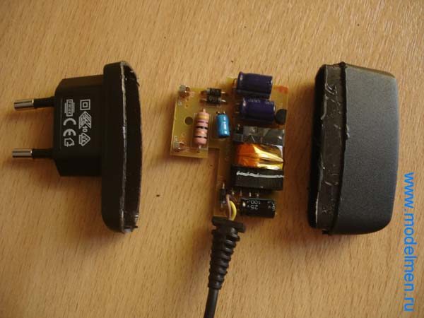
There were several parts on the back of the board; the circuit turned out to be not so simple, but still not so complicated that you couldn’t fix it yourself.

Below in the photo are the contacts of the inside of the case.

There is no step-down transformer in the charger circuit; its role is played by an ordinary resistor. Next, as usual, a couple of rectifying diodes, a pair of capacitors for rectifying the current, then comes a choke and finally a zener diode with a capacitor completes the chain and outputs the reduced voltage to a wire with a connector to the mobile phone.

The connector has only two contacts.