Electrical circuit diagram of a homemade laboratory power supply. Laboratory power supply: master class on how to make a simple device with your own hands
For setting up, repairing automotive electronic and radio devices or charging batteries must have good source nutrition.
Use of modern circuit technology and element base allow you to make a power source at home, which in its basic technical characteristics is not inferior to the best industrial designs.
Basic requirements that such a power source must satisfy:
- voltage adjustment in the range 0 - 25 V;
- ability to provide load current up to 7 A with minimal ripple;
- adjustment of current protection operation. In addition, the operation of the current protection must be fast enough to prevent damage to the source itself in the event short circuit on the way out.
The ability to smoothly adjust the current limit in the power supply allows you to configure external devices prevent their damage. All these requirements are satisfied by the proposed universal power supply circuit. Besides, this block power supply allows you to use it as a source of stable current.
Basic technical specifications power supply:
- smooth voltage adjustment in the range from 0 to 25 V;
- ripple voltage, no more than 1 mV;
- smooth adjustment of current limitation (protection) from 0 to 7 A;
- voltage instability coefficient is not worse than 0.001%/V;
- current instability coefficient is not worse than 0.01%/V;
- The source efficiency is no worse than 0.6.
Schematic diagram
The electrical circuit of the power supply consists of a control circuit, a transformer (T1), a rectifier (VD4 - VD7), power control transistors VT3, VT4 and a switching unit for transformer windings.
The control circuit is assembled on two universal operational amplifiers (op-amps), located in one housing, and is powered by a separate transformer T2. This allows the output voltage to be adjusted from zero to more stable work the entire device.
For relief thermal regime For the operation of power control transistors, a transformer with a sectional secondary winding is used. The taps are automatically switched depending on the output voltage level using relays K1, K2. What allows, despite high current in load, apply heat sink for VT3 and VT4 comparatively small sizes, and also increase the efficiency of the stabilizer.
The switching unit is designed to, using only two relays, ensure switching of four taps of the transformer; it turns them on in the following sequence: when the output voltage exceeds the level of 6.2 V, K2 turns on; when the level of 15.3 V is exceeded, K1 is turned on (in this case, the maximum voltage is supplied from the transformer windings).
The specified thresholds are set by the zener diodes used (VD10, VD12). The relay is turned off when the voltage drops negative sequence, but with a hysteresis of approximately 0.3 V, i.e. when the voltage drops by this value lower than when turned on, which eliminates chatter when switching windings.
The control circuit consists of a voltage stabilizer and a current stabilizer. If necessary, the device can operate in any of these modes. The mode depends on the resistance of the regulators "I" (R21, R22). The voltage stabilizer is assembled on elements DA3, VT5, VT6.
Rice. 1. Schematic diagram laboratory source power supply with current limiting adjustment.
The stabilizer circuit works as follows. Necessary output voltage set by resistors “roughly” (R9) and “finely” (R10). In voltage stabilization mode, the signal feedback voltage (-Uoc) from the output (X2) through a divider of resistors R9, RIO, R11 is supplied to non-inverting input 2 operational amplifier DA3.
A reference voltage of +9 volts is supplied to the same input through resistors R3, R5, R7. When the circuit is turned on, the positive voltage at output 12 DA3.1 will increase (it comes to control VT4 through transistor VT5) until the voltage at the output terminals X1 and X2 reaches the level set by resistors R9, R10.
Due to the negative voltage feedback coming from output X2 to input 2 of the DA3.1 amplifier, the output voltage of the power supply is stabilized. In this case, the output voltage will be determined by the relationship:
where Uop = + 9 V.
Accordingly, by changing the resistance of resistors R9 “roughly” and R10 “precisely”, you can change the output voltage (Uout) from 0 to 25 V. When a load is connected to the output of the power source, a current begins to flow in its output circuit, creating a positive voltage drop across resistor R23 (relative to the common wire of the circuit).
This voltage is supplied through resistor R21, R22 to the connection point R8, R12. A reference negative voltage of 9 volts is supplied from the zener diode VD9 through R6, R8.
The DA3.2 operational amplifier amplifies the difference between them. While the difference is negative (i.e., the output current is less than the value set by resistors R23, R24), + 15 V operates at output 10 DA3.2. Transistor VT6 will be closed and this part of the circuit does not affect the operation of the voltage stabilizer.
When the load current increases to a value at which a positive voltage appears at input 7 of DA3.2, there will be a negative voltage at output 10 of DA3.2 and transistor VT6 opens slightly. A current will flow in circuits R16, R17, HL1, which will reduce the opening voltage based on the regulating power transistor VT4.
The glow of the red LED (HL1) indicates that the circuit has entered current limiting mode. In this case, the output voltage of the power supply will decrease to a value at which the output current will have a value sufficient for the current feedback voltage (Uoc) taken from resistor R10 and the reference voltage at the connection point R8, R12, R22 to mutually were compensated, i.e., zero potential appeared.
As a result, the output current of the source will be limited at the level specified by the position of the slider of resistors R21, R22. In this case, the current in the output circuit will be determined by the relation:
where Uop = - 9 V.
Diodes (VD11) at the inputs of operational amplifiers protect the microcircuit from damage if it is turned on without feedback or if the power transistor is damaged. In operating mode, the voltage at the inputs of the op-amp is close to zero and the diodes do not affect the operation of the device.
Capacitor C8 limits the band of amplified op-amp frequencies, which prevents self-excitation and increases the stability of the circuit.
Settings
With error-free installation in the control unit circuit, you will only need to adjust the maximum output voltage adjustment range 0: 25 V with resistor R7 and the maximum protection current of 7 A with resistor R8.
The switching unit does not need to be configured. It is only necessary to check the switching thresholds of relays K1, K2 and the corresponding increase in voltage on capacitor C3.
When the circuit is operating in voltage stabilization mode, the green LED (HL2) lights up, and when switching to current stabilization mode, the red LED (HL1) lights up.
Details
Trimmer resistors R7 and R8 are SPZ-19a type; variable resistors R9, R10, R21, R22 - type SPZ-4a or PPB-1 A; fixed resistors R23 - type C5-16MV for 5 W, the rest are from the MLT or C2-23 series of appropriate power.
Capacitors C6, C7, C8, SYU type KIO-17, electrolytic capacitors C1 - C5, C9 type K50-35 (K50-32). The DA1 chip can be replaced with an imported analogue 78L15; DA2 - on 79L15; DA3 on rA747 or two 140UD7 microcircuits.
LEDs HL1, HL2 are suitable for any different colors glow. Power transistors are installed on a radiator with an area of about 1000 cm^2.
Two power transistors are installed in parallel to ensure reliable operation of the device in the event of a short circuit at the output terminals.
In the worst case, power transistors must briefly withstand power overload P = Ubx*I = 25x7 = 175 W. And one KT827A transistor can dissipate power no more than 125 W. Diodes VD4 - VD7 must be installed on a small radiator.
Relays K1, K2 are used in standard size R-15 (Polish production) with a winding on operating voltage 24 V (winding resistance 430 Ohm) - due to their unframed design, they have small dimensions and sufficiently powerful switching contacts. You can also use domestic relays such as REN29 (0001), REN32 (0201).
Switching voltage from transformer T1, relays K1 and K2 are inertial and do not provide an instantaneous reduction in the voltage coming from the secondary winding of T1, but they will reduce the thermal dissipation of power on the power transistors when long work source.
Microammeter RA1 is a small-sized type M42303 or similar with an internal shunt for a current of up to 10 A. For ease of operation of the power source, the circuit can be supplemented with a voltmeter indicating the output voltage.
An industrial transformer type TPPZ19-127/220-50 is used as a network transformer T1. T2 - type TPP259-127/220-50. The transformer can be made independently on the basis of an industrial transformer with a power of 200 W, winding all the windings (T1 and T2) on one transformer.
About once a year, an inexorable desire awakens in me to make a laboratory power supply (for example, I described my last laboratory). And then they offered to review something - well, I couldn’t resist, because I’ve wanted to try this module for a very long time. Unfortunately, there will be no dismemberment, because the structure is extremely difficult to disassemble, and I was afraid not to assemble it properly in reverse. :)
There was already a similar module, but this one attracted me with its display. Still, large numbers are much more convenient than small ones.
I will start, however, not with the main character of the review, but with the second, no less important one (also provided for review), without which this module is useless. 

The power supply is somewhat different from the original version, and, unfortunately, not for the better. External differences consist in the inscription ac-dc 24v instead of 2412DC on the original version, and the presence of a certain website address on the bottom side of the board. The “internal” differences are much more interesting. But first, the appearance.
The main problem of this copy (or rather the entire batch) is the low-quality output connector. it is completely disgustingly soldered, and naturally poorly soldered. You need to solder it right away, because it barely holds on. However, as I wrote, this is a problem of an instance or a batch, and in general, the likelihood of this problem repeating among other buyers after some time is not so great. 
In general, soldering is not very neat, and it is advisable to inspect the board and solder suspicious areas 

The famous capacitor is sealed as usual as before, and it is also advisable to replace it, as the respected Kirich wrote. He also recommends hanging ceramics along the outlet and parallel to the output electrolytes. 
The snubber diode, however, is soldered correctly: 
The board is well washed, and in general everything is fine with it, if not for one small BUT. It seems that the manufacturer of the PWM controller on which this power supply is assembled decided to improve the “green” mode, and instead of reducing the frequency by light load- produces packets of pulses at the standard 62-64 kHz to the gate of the power transistor. It looks on the oscillator as a short burst of control pulses and a long pause - about 30 mS (when working without load), and with increasing load these pauses decrease. And everything would be fine, if not for that very small BUT - as a result, we end up with a fair amount of “saw”:


In the photo - operation without load and with a one-amp load seems to be the case. AC 0.2V/div and 5mS/div.
It seems that my thoughts above are correct, and this is such an interesting “feature” of new versions of the power supply. The old ones, as they said, significantly reduced the frequency - down to 14-15 kHz, but these ones begin to work “pulse” and produce a saw output. It’s not entirely clear to me how to deal with this - I also tried installing capacitors of larger capacity - but it didn’t work.
Naturally, advice on improvements is welcome in the comments, because now it seems that all power supplies come with such a “feature,” at least in the comments to Kirich’s review I came across similar oscillators.
However, oddly enough, in the end everything works quite normally.
Well, let's move on to the main character?
Supplied in a clear plastic box, wrapped in instructions. The instructions are large, on good paper, in Chinese and quite sane English.


As you can see, the stated accuracy is 0.5%, and I must say that it fully provides it, although at very low currents it lies, which, however, is natural - but this is lower.
The module itself is compact (window dimensions in the housing for installation are 39x71.5, plus samples up to 75.5, depth 35.5), display 28x27, digit height 5mm (on a “regular” ampere-voltmeter 7.5mm). The display itself is bright, contrasty, with good viewing angles. The only thing I don’t really like is the rather slow update (the readings are probably updated twice a second). But I think this is not a problem with the display, but with the firmware, and it doesn’t bother me at all.


On the 8-legged microchip it says XL7005A - PWM controller 150 kHz 0.4A
Unfortunately, to disassemble it - non-trivial task, because three boards are soldered together in a “sandwich”, three connectors with 8 contacts, which are quite tight, and you can easily touch something and ruin it. so sorry. Above the encoder you can see the inscriptions rx gnd tx - apparently the module supports data transfer, and above that there is clearly a connector for flashing. In general, the build quality left a pleasant impression. The flux is not washed off in the places where the transition contacts are soldered, which is natural and understandable, and the flux is clearly such that it does not require washing off.
It is clear that such a module is purchased not for disassembly, but for assembly, and not for what, but the power supply. For those who do not know what a laboratory power supply is and why it is needed, I will briefly write what it is adjustable block power supply, with output current limitation and output voltage regulation. It is needed to power devices “on the table”, for example during repair or development. It prevents you from accidentally burning something;) You can also charge batteries with it, for example.
Let's move on to assembling the power supply. Perhaps I’ll hide it under a spoiler, otherwise there will be a lot of photos.
power supply assembly
We will assemble it in the Kradex Z-3 case. all the components fit into it so well that it seems that they were simply created for each other. ;)
Kradex cases are distinguished by the idiotic design of the connecting posts - they are too far from the side walls and too close to the front and rear. Therefore, we mercilessly bite them out and move them to the middle of the building, where they will not disturb anyone. We fix it with dichloroethane. Similarly, we make racks for attaching the power supply.

Next, we mill the front and back panel, as well as holes for the fan. in principle, it’s not really needed, but I decided to install it right away so as not to have to get up twice. Unfortunately, there was only enough space for a 50mm fan.


Since there will be a USB connector on the “face,” we solder textolite “ears” to it, and glued pieces of plastic with pre-cut M3 threads to the body. the shortest screws “from the computer” are perfect for attaching the connector to the front panel.
I don’t know that you need to clamp the cutter into the chuck, and there is a fan chuck, and the collets are good, but I’m a slob, and the material here is soft, so I’m too lazy to put in another chuck and I mill small things like that.
For USB power supply and the fan, I used converters from my previous review, gluing them to a radiator made of an 8x15 w-shaped profile. greatly improves cooling. The fan is powered from 6.5V - at 5V it blows very weakly. I wanted to add a speed control, but I was too lazy, and decided that a separate converter would be enough for manual installation any speed you like.

I decided to modify the “primary” power supply - slightly increase the voltage in order to get at least 24V at the output of the entire device. Taking into account the limitation of the maximum input voltage of the used converters to 28V, I decided to “overclock” the power supply to 26V. To do this, solder a 22 kOhm resistor parallel to resistor R19.


Well, the result:


Now let's move on to testing.
First of all, how does it work? top small line - set values current and voltage. large numbers are the measured values at the output, and below - input voltage(minimum difference between input and output is about a volt). The icons on the right show the current status: blocking, status (ok/not ok), output mode (cc/cv) and output status - on/off. When turned on, the output is turned off. Turn the output on and off using the button under the encoder. The icon is off - red, on - green. Locking by long pressing the encoder.


When we press the set button, we have the opportunity to change the current current and voltage values. the variable digit is highlighted in red in top line, and switches by pressing the encoder. Rotating the encoder changes the value. when moving from 9 to 0, the most significant digit increases.

When you press set again, we get to the “advanced” settings menu. And in the top line, accordingly, they begin to display current parameters output - current and voltage.

Here we have the output voltage, output current, voltage/current/power of the protection, backlight brightness, and the current memory cell. There are 10 of these cells. M0 is the “manual” mode, that is, what we are dabbling in now. these values are saved and restored the next time you turn them on.
Select a parameter using the up/down buttons, then press the encoder and change the parameter, exit with the set button. in order to save values to some memory cell, you must first select it in lower point menu, then change everything you need, and then go to the cell number in the bottom menu item and hold the set button for two seconds. The number of the cell in which it was saved will appear on the left between the icons.

On|off in the lower menu item on the right is the output state when selecting this memory cell. off - turned off, on - “as it was.”
The controls are, of course, a little strange. To be honest, I still don’t understand how these “protections” work; I simply use them in current limiting and voltage stabilization mode.
Next. the next press of the set button takes us to “ home screen" The selection of a memory cell is carried out either by holding the up button to select M1, or the down button to select M2, or the set button - and then use the encoder to select the cell number. It’s a shame that when switching memory cells, the current and voltage stored there are not displayed. It would be logical and convenient - but no.
Now - measurements. I put it in a table, and, to be honest, I won’t even really count and comment, because the pot is no longer cooking something;) Set is what we set, meas is what it measures at its output, tester is what it shows accordingly tester. At low currents it lies quite significantly, but IMHO this is forgivable. From 100mA and above - it consistently lies at 3mA (underestimates), at lower currents - not so much, but it also lies. In my opinion, the error at adequate currents varies (0.5% +2 digits). Let the metrologists correct it if anything;) At low currents, of course, it’s a miss.

Oh, I almost forgot. interference and ripple measurements.
At low currents: 
At high (2.5A it seems) currents: 
AC 0.2V 500µS.
When turned on, the voltage gradually increases, turns on in CC mode, then switches to CV mode: 
If you connect the LED and then turn on the output, it lights up for approx. If you first turn on the output and then connect the LED, it doesn’t even have time to make a sound, it burns out instantly, which is predictable.
To sum it up: I really like it. IMHO for this money (up to 50 bucks) there are simply no alternatives. In terms of work, IMHO he will be no worse than any other Chinese laboratory worker. It’s not the most thoughtful control, but it’s not all that scary either - I think you can get used to it quickly enough, and what’s there to really control... you set it up once and be happy, but then turning the voltage is a matter of the button and the encoder. According to the design of the power supply, I’m no longer sure that the sockets should have been made on the left, perhaps it was worth moving them to the right - which, however, can be done simply by turning the front panel over. Undoubtedly, in the comments they will throw out links to cheaper options, but even for this amount, everything is quite good.
The product was provided for writing a review by the store. The review was published in accordance with clause 18 of the Site Rules.
I'm planning to buy +90 Add to favorites I liked the review +53 +127For food various schemes you need different power supplies with different voltages and currents, for such purposes the workshop requires an regulated power supply, that is, a laboratory power supply. The prices for such devices are quite impressive and therefore you will have to assemble a laboratory power supply with your own hands. From what I have in my bins I will get a good device with an output of up to 18V and a current of up to 2.5A; a digital voltmeter that just arrived from China will be suitable for indication, but first things first.
Firstly, the maximum output parameters were selected due to the available free transformer from stereo speakers 2*17V 2A. windings are connected in parallel. After the diode bridge with capacitors, the voltage will increase to approximately 24V. It must be taken into account that the voltage should be with reserve. A drop of a few volts on the transistors, plus under load it will still drop by a few volts, 19V will remain clean, so 18V is a stable maximum that can be squeezed out. The load of 2.5A was chosen so as not to heavily load the transformer windings; in this mode, the transformer will feel better, because it will be loaded by 70-80%. I figured out what to eat, now what to eat
Now it's time to choose a scheme for laboratory block nutrition. The circuit was selected, assembled and tested; it is a simple and affordable laboratory power supply (LPDP) V14. The circuit was taken from the Soldering Iron forum and slightly modified to suit its output voltages and currents
An overcurrent indicator is assembled on DA1.3. When there is a current limit, this indicator indicates this
To measure the load current, a voltage amplifier is assembled on DA1.4, recalculated to a gain of 5 times. When the load is maximum across resistor R20 there is a drop of 0.5V, this voltage is amplified and at the output of the op-amp there is a voltage equal in value to the current consumption.
Well, the heart of the circuit is assembled on the first two comparators. This is a current stabilizer that controls a voltage stabilizer. I assembled something similar, only in the circuit the current and voltage were controlled independently. I won’t describe in detail how sequential connection of stabilizers works, you can read about parallel connection in the article, the operating principle is similar.
In the circuit, R12R14 was recalculated for an output voltage of 18V, and R11 for voltage regulation was replaced by 5k. R20 is recalculated for a current of 2.5A, at the maximum current at R20 there should be a drop of 0.5V. R20 is calculated using a simple formula from Ohm’s law R20=0.5(V)\Imax(A)
To make the circuit a little more practical, I added a protection circuit against short circuits and reverse polarity. This scheme has proven itself well and I sculpt it anywhere))
In short, I decided what I would use where. I collected all the components in a heap, separated printed circuit board and soldered everything

As you can see, the output transistors were used in parallel connection. Total power dissipation 120W, maximum current 20A, breakdown voltage 60V. Both transistors are wired to a common radiator outside the case. By the way, the case was used from an old plastic music speaker

The printed circuit board is ready, the case is there. transistors on the radiator. The time has come to finally decide what tasks will be performed by the laboratory power supply and install the front panel. I will draw the panel in SPL6. 
On the panel I will place a voltmeter, voltage and current regulator.
Switch measuring volts and amperes.
Two indicators for overload and short circuit protection
Switch between diode bridge output and LBP output
Switch between LBP and charger. Negative output either with LBP or with protection against polarity reversal and short circuit
Now knowing what will be where, you can put it together general scheme laboratory power supply and spread braids of wires from the board to the front panel. This is what happened

 I think it's time to put everything back into the case
  Here is a photo of the finally assembled board
And this is what everything looks like in the case. 

After assembling everything into the case, you can try to plug the laboratory power supply into a power outlet. Output 18.5V  The first switching on of the laboratory power supply under a load of 50% as a load on the engine from a 12V screwdriver. By the way, the overload indicator shows that the power supply is in current limiting mode. On the indicator the current consumption is 1.28A
 This is the laboratory power supply I got:
I used a voltmeter from China as an indicator, having previously modified it. The voltmeter also indicated the voltage from which it was powered, I decided to separate these channels so that it would be possible to measure from 0V to 20V. I removed the resistor connecting the power and voltage measurement contacts, it is marked in red in the photo. Powered the indicator from reference voltage 12V circuits 
This voltmeter can be ordered on AliExpress. here is the link
If you need test results for this block, please write in the comments.
With uv. Edward
Support new projects with a coin, scroll down the page, be kind.
Good afternoon. Let me present to your attention a simple and reliable laboratory power supply. I assembled it about 10 years ago, so I don’t remember in which magazine I found its diagram. It is distinguished by its simplicity, reliability, and most importantly, it allows you to regulate the output voltage within the widest range: up to 40 volts! Agree, how often this is what is missing high voltage, for experiments and experiments with REA. And it is surprising that many industrial laboratory power supplies are unable to output more than 20V - this significantly limits their scope of application.
The LBP circuit diagram consists of a transformer (T1), a diode bridge (VD1-VD4), a parametric voltage stabilizer on the elements (VD6, VD8, HL1, R1, R2, R3), a flow current limiter (VT3, R7, R8, R9) with Possibility of short circuit protection (L1, VD7, R6) because the choke delays the instantly increasing current during a short circuit for the time required for the current limiter to start operating.

Transistor VT1 is a disconnector for the parametric voltage stabilizer and current limiter units, VT2 amplifies the output current of these units to the value necessary to control VT4. The transformer was used with a secondary winding of 28 volts 1.5 amperes.

The diode bridge used KVRS5010, and the KT808AM transistor was used as VT4. Instead of resistor R8, I installed an assembly of eight resistors (at the bottom of the diagram I drew how they are connected), which I wrapped with blue electrical tape and glued on top of the voltmeter.

I used resistors R14 and R15 with a resistance of 470 ohms. The L1 inductor without a core contains 150 turns; I used my little finger as a mandrel, wound the turns “in bulk”, after winding, carefully removed it from the little finger and filled it with hot glue.

Setting up LBP
Almost no adjustment is required; it is enough to select only the resistance of resistor R8 to limit the maximum current to the desired level. My current is limited to 350 milliamps, which is quite enough to power most homemade products.

I have charged this power supply several times. lithium batteries from cell phones, you know, it’s very convenient, I turned the output voltage up to 10 volts, connected the battery, and when the voltage on the voltmeter rose to about 4.2 volts, the battery was charged. But it is advisable to control the process, since LI-Ion battery Explosive when overcharged. See a short video showing it in action below:
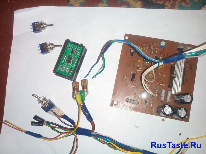
Need for laboratory power supply with the ability to adjust the output voltage and the protection threshold for load current consumption arose a long time ago. Having worked through a bunch of material on the Internet and gained some insight into own experience, settled on the following design. The voltage regulation range is 0-30 Volts, the current supplied to the load is determined mainly by the transformer used, in my version I can easily draw more than 5 Amperes. There is an adjustment of the protection threshold for the current consumed by the load, as well as against a short circuit in the load. The indication is performed on the LSD16x2 LCD display. I think the only drawback of this design is the impossibility of transformation this source power supply to bipolar and incorrect indication of current consumption by the load in the case of combining the poles - together. My goals were to power mainly unipolar power supply circuits, so even two channels, as they say, head on. So, the diagram of the display unit on the MK with its functions described above:
Current and voltage measurements I - up to 10 A, U - up to 30 V, the circuit has two channels, the photo shows voltage readings up to 78L05 and after, it is possible to calibrate for existing shunts. There are several firmware for ATMega8 on the forum, but not all have been tested by me. The circuit uses the MCP602 microcircuit as an operational amplifier, its possible replacement- LM2904 or LM358, then you need to connect the op-amp power to 12 volts. On the board, I replaced the diode at the input of the stabilizer and the power choke with a jumper; the stabilizer must be placed on a radiator - it heats up significantly.

For correct display current values, it is necessary to pay attention to the cross-section and length of the conductors connected from the shunt to the measuring part. The advice is this: minimum length, maximum cross-section. For the laboratory power supply itself, a circuit was assembled:

It started up immediately, the output voltage adjustment is smooth, as well as the current protection threshold. The print had to be adjusted to LUT, this is what happened:
Connecting variable resistors:

Location of elements on the power supply board
Pinout of some semiconductors

List of laboratory IP elements:
R1 = 2.2 KOhm 1W
R2 = 82 Ohm 1/4W
R3 = 220 Ohm 1/4W
R4 = 4.7 KOhm 1/4W
R5, R6, R13, R20, R21 = 10 KOhm 1/4W
R7 = 0.47 Ohm 5W
R8, R11 = 27 KOhm 1/4W
R9, R19 = 2.2 KOhm 1/4W
R10 = 270 KOhm 1/4W
R12, R18 = 56KOhm 1/4W
R14 = 1.5 KOhm 1/4W
R15, R16 = 1 KOhm 1/4W
R17 = 33 Ohm 1/4W
R22 = 3.9 KOhm 1/4W
RV1 = 100K trimmer
P1, P2 = 10KOhm
C1 = 3300 uF/50V
C2, C3 = 47uF/50V
C4 = 100nF polyester
C5 = 200nF polyester
C6 = 100pF ceramic
C7 = 10uF/50V
C8 = 330pF ceramic
C9 = 100pF ceramic
D1, D2, D3, D4 = 1N5402,3,4 diode 2A - RAX GI837U
D5, D6 = 1N4148
D7, D8 = 5.6V Zener
D9, D10 = 1N4148
D11 = 1N4001 diode 1A
Q1 = BC548, NPN transistor or BC547
Q2 = 2N2219 NPN transistor
Q3 = BC557, PNP transistor or BC327
Q4 = 2N3055 NPN power transistor
U1, U2, U3 = TL081
D12 = LED
The finished boards look like this in my version:

I checked it with the display, it works fine - both a voltmeter and an ammeter, the problem here is different, namely: sometimes there is a need for a bipolar supply voltage, I have separate secondary windings of the transformer, you can see from the photo there are two bridges, that is, two completely independent ones from another channel. But the measurement channel is common and has a common minus, therefore it will not be possible to create a middle point in the power supply, due to the common minus through the measuring part. So I’m thinking of either making each channel its own independent measuring part, or maybe it’s not very often that I need a source with bipolar power supply and a common zero... Next, I present the printed circuit board, the one that has been etched so far:

After assembly, first thing: set the fuses exactly like this:

Having assembled one channel, I verified its functionality:


While the left channel of the measuring part is turned on today, the right one is hanging in the air, therefore the current shows almost maximum. I haven’t installed the cooler for the right channel yet, but the essence is clear from the left one.

Instead of diodes for now in the left channel (it is below the right board) of the diode bridge that during the experiments I threw out, although 10A, I installed a 35A bridge on the radiator under the cooler.

The wires of the second channel of the transformer secondary are still hanging in the air.

Bottom line: the stabilization voltage jumps within 0.01 volts over the entire voltage range, the maximum current that I could draw was 9.8 A, which was enough, especially since I expected to get no more than three amperes. The measurement error is within 1%.
Flaw: I can’t transform this power supply into a bipolar one due to the general disadvantage of the measuring part, and after thinking I decided that I couldn’t configure the terminals, so I abandoned the scheme of completely independent channels. Another disadvantage, in my opinion, of this measuring circuit is that if we connect the poles together at the output, we lose information about the current consumption by the load due to the common body of the measuring part. This happens as a result of paralleling the shunts of both channels. And in general source The food turned out not bad at all and will be available soon. Author of the design: GOVERNOR
Discuss the article DIAGRAM OF LABORATORY POWER SOURCE