PCI devices - what are they? PCI video card.
♦ MEMR# (MRDC#) - read memory in any area up to 16 MB.
♦ OWS# (SRDY#, NOWS#, ENDXFR) - shortening the current cycle at the initiative of the addressed device.
♦ MASTER* (MASTER 16#) - request from a device using 16-bit DMA channel for bus control. Upon receipt of the DACK acknowledgment, the Bus-Master can seize the bus.
On the EISA bus additional contacts slots (not available to ISA cards) there is an expansion of data and address buses up to 32 bits, as well as a set of signals that ensure data transmission in synchronous mode with the possibility of burst cycles.
6.2. PCI bus
PCI (Peripheral Component Interconnect) local bus - the peripheral component connection bus is the main expansion bus modern computers. It was designed with the Pentium in mind, but also worked well with 486 processors. PCI is now a clearly standardized, high-performance and reliable expansion bus. The first version of PCI 1.0 appeared in 1992. PCI 2.0 (1993) introduced a specification for connectors and expansion cards. Version 2.1 (1995) introduced a frequency of 66 MHz. Currently, the PCI 2.2 specification is in force (December 1998), which clarifies and clarifies some provisions of the previous version 2.1. This description Based on the text of the PCI Local Bus Specification standard. Revision 2.2" dated December 17, 1998, published by the PCI SIG (Special Interest Group).
At first, the PCI bus was introduced as an extension (mezzanine bus) to systems with a main ISA bus, later becoming the central bus: it is connected to the processor system bus by a high-performance (“north” bridge) included in the chipset motherboard. The remaining I/O expansion buses (ISA/EISA or MCA), as well as the local ISA-like X-BUS bus and the LPC interface, to which the system board chips are connected (ROM BIOS, interrupt controllers, keyboards, DMA, COM and LPT ports, NGMD and other “little things”) are connected to the PCI bus via the “south” bridge. In modern motherboards with hub architecture, the PCI bus has been moved to the periphery, without compromising the power of the communication channel with the processor and memory, but also without loading devices on other buses with transit traffic.
The bus is synchronous - all signals are captured by the positive edge (edge) of the CLK signal. The nominal synchronization frequency is considered to be 33 MHz; if necessary, the frequency can be lowered (on machines with a 486 processor, frequencies of 20-33 MHz were used). In many cases, the frequency is successfully overclocked to 41.5 MHz (half the typical frequency system bus 83 MHz). Starting from version 2.1, it is possible to increase the frequency to 66 MHz with the consent of all devices on the bus. The nominal width of the data bus is 32 bits, the specification also specifies an extension of the bit width to 64 bits. At bus frequency 33 MHz theoretical throughput reaches 132 MB/s for a 32-bit bus and 264 MB/s for a 64-bit bus; at a synchronization frequency of 66 MHz - 264 and 528, respectively. However, these peak values are reached only during packet transmission, and due to protocol overhead, the actual average total (for all masters) bus throughput is lower.
The processor can interact with PCI devices by commands accessing memory and I/O ports addressed to the areas allocated to each such device during configuration. Devices can generate requests for masked and non-maskable interrupts. There is no concept of DMA channels for the PCI bus, but the bus agent itself can act as a master, supporting high-performance exchange with memory (and not only) without taking up resources
central processor. Thus, for example, exchange in DMA mode can be implemented with AT A devices connected to the PCI IDE controller (see clause 9.2.1). PCI specification requires devices to be able to move all occupied resources within the available addressing space. This allows for conflict-free resource allocation across many devices (functions). To control devices, it is recommended to use memory cells instead of I/O ports whenever possible. Same thing functional device can be configured in different ways, mapping its registers to either memory space or I/O space. The driver can determine current setting by reading the contents of the register base address device, - the sign of the I/O space will be the single value of bit 0 (see clause 6.2.12). The driver can also determine the interrupt request number that is used by the device.
6.2.1. PCI Device Addressing
For the PCI bus, a hierarchy of addressing concepts has been adopted: bus, device, function. These concepts appear only when accessing configuration space registers (see section 6.2.12). These registers are accessed at the configuration stage - re-accounting of detected devices, allocating non-overlapping resources to them (memory areas and I/O space) and assigning hardware interrupt numbers. With further regular work devices will respond to requests at their assigned memory and I/O addresses, communicated to the associated software modules. These addresses are received from the AD bus at the beginning of each transaction. Separate IDSEL lines are used to access the configuration space. A PCI device is a chip or expansion card connected to one of the PCI buses and using a dedicated IDSEL line belonging to this bus for identification. The device can be multifunctional, that is, consist of many (from 1 to 8) so-called functions. Each function is allocated a configuration space of 256 bytes (see section 6.2.12). Multifunction devices should only respond to configuration cycles with function numbers for which configuration space is available. In this case, function number 0 must be present; the numbers of other functions are assigned arbitrarily by the device developer (in the range 1-7). Simple (single-function) devices, depending on the implementation, can respond either to any function number or only to function number 0.
PCI bus is a set of signal lines (see section 6.2.2) directly connecting the interface pins of a group of devices (slots, microcircuits on the system board). The system may have several PCI buses connected by PCI bridges (see clause 6.2.10). Bridges electrically separate the interface signals of one bus from another, connecting them logically; The main bridge connects the main bus to the system core (processor and memory). Each bus has its own bus number (PCI bus number). Tires are numbered sequentially; the main bus is numbered zero.
From a configuration point of view, the minimum addressable unit of this hierarchy is a function; her full address consists of three parts: bus number, device number and function number. Short form Identification of the form RSY:1:2 (for example, in Unix OS messages) means function 2 of device 1 connected to the main (0) PCI bus.
The PCI bus adopts geographic addressing - the device number is determined by the location of its connection. The device number (device number or dev) is determined by the AD bus line to which the IDSEL signal line of this slot is connected: kADU - devO(MOCT),AD12-devl,...AD31 -dev20. In neighboring PCI slots, as a rule,
neighboring device numbers are used; their numbering is determined by the developer of the motherboard (or passive backplane in industrial computers). Often for
slots use descending device numbers, starting from 20. Groups of adjacent slots can be connected to different buses; on each PCI bus the numbering of devices is independent (there may be devices with the same dev numbers, but different numbers tires). PCI devices integrated on the motherboard use the same addressing system. Their numbers are “tightly soldered”, while the addresses of expansion cards can be changed by moving them to different slots. One PCI card can only contain one bus device to which it connects, since only one IDSEL line is allocated to it in the slot. If several devices are placed on the card (for example, a 4-port Ethernet card), then you have to install a bridge on it
This is also a PCI device, which is accessed via the IDSEL line allocated to this card. This bridge organizes an additional PCI bus on the card, to which many devices can be connected.
From the point of view of accessing memory and I/O spaces, the geographic address (bus and device number) is indifferent (not taking into account the performance differences associated with connecting devices to different PCI buses). However, the device number determines the number of the interrupt request line that the device can use. For more information about this, see paragraph 6.2.6; here we note that on the same bus, devices with numbers different from each other by 4 will use the same interrupt line. The ability to route them to different interrupt lines can only appear if they are on different buses (this depends on the motherboard).
You can simply figure out the numbering of devices and the interrupt lines they receive on a specific board: install one PCI card in each slot one by one (turning off the power) and look at the messages about detected PCI devices displayed on the display at the end of the POST test. These messages will also include PCI devices installed directly on the system board (and not disabled). CMOS parameters Setup).
But so that there are no illusions of simplicity and transparency, we note that “particularly smart” operating systems (Windows) are not satisfied with the received assignments of interrupt numbers and change them at their own discretion (which cannot in any way affect the separability of lines).
6.2.2. PCI bus protocol
Each transaction (exchange on the bus) involves two devices - the initiator of the exchange, also known as the master device, and the target device, also known as the slave. The PCI bus treats all transactions as packets: each transaction begins with an address phase, which can be followed by one or more data phases. The composition and purpose of the bus interface signals are given in Table. 6.11.
Table 6.11. PCI bus signals | ||
Purpose | ||
Address/Data - multiplexed address/data bus. At the beginning of the transaction, the address is transmitted to |
||
subsequent cycles-data | ||
Command/Byte Enable - command/permission to access bytes. Command that determines the queue type |
||
bus cycle, specified by a four-bit code in the address phase | ||
Frame. The introduction of a signal marks the beginning of the transaction (address phase), the removal of the signal indicates that |
||
the subsequent data cycle is the last in the transaction |
||
Device Select- device selected (CP response to transaction addressed to it) |
||
Initiator Ready - readiness of the master device for data exchange |
||
Target Ready - readiness of the control center for data exchange | ||
Request to the master to stop the current transaction |
||
Bus capture signal to ensure consistent operation. Used by a bridge for which |
||
multiple PCI transactions are required to complete one operation |
||
Request - request from the master device to seize the bus | ||
Grant - granting bus control to the master |
||
Parity - common parity bit for AD and C/BE# lines |
||
PRSNT# Present - board presence indicators encoding the power consumption request. On the expansion card, one or two LED lines are connected to the GND bus, which is sensed by the motherboard
Reset - reset all registers to their initial state |
|
Initialization Device Select - device selection in configuration cycles |
|
reading and writing |
|
System Error - system error. Data address parity error in special loop or other |
|
catastrophic error detected by the device. Activated by any PCI device and causes |
|
Request 64 bit - request for a 64-bit exchange. The signal is input 64-bit |
|
initiator, it coincides in time with the FRAME* signal. During reset completion (signal |
|
RST*) signals to a 64-bit device that it is connected to a 64-bit bus. If 64-bit |
|
If the device does not detect this signal, it must be reconfigured to 32-bit mode by disabling |
|
high byte buffer circuits |
|
Confirmation of 64-bit exchange. The signal is input by the 64-bit CPU, which has recognized its address, simultaneously with |
|
DEVSEL*. The absence of this confirmation will force the initiator to perform the exchange in 32-bit |
INTA#, INTB*, Interrupt A, B, C, D - interrupt request lines, level sensitivity, INTC#, INTD* active level - low, which allows separability (sharing) of lines
Purpose | ||
Snoop Done - signal that the snoop cycle is complete for the current transaction. Low level indicates |
||
incompleteness of the cache memory coherence monitoring cycle. Optional signal, used only |
||
devices and buses with cached memory |
||
Snoop Backoff - hit of the current memory access of the bus subscriber |
||
to the modified cache line. Optional signal, used only by subscribers on the cacheable bus |
||
memory with write-back algorithm |
||
Test Clock - JTAG test interface synchronization |
||
Test Data Input - JTAG test interface input data |
||
Test Data Output - JTAG test interface output data |
||
Test Mode Select- mode selection for the JTAG test interface |
||
Test Logic Reset - reset test logic |
||
At any given time, the bus can only be controlled by one master device, which has received the right to do so from the arbiter. Each master device has a pair of signals - REQ# to request bus control and GNT* to confirm that bus control has been granted. The device can start a transaction (set the FRAME* signal) only when the received GNT* signal is active. Removing the GNT* signal prevents the device from starting the next transaction, and under certain conditions (see below) causes it to terminate the current transaction. Arbitration of requests to use the bus is handled by a special node included in the motherboard chipset. The priority scheme (fixed, round-robin, combined) is determined by the arbiter programming.
Common multiplexed AD lines are used for address and data. Four multiplexed C/BE lines provide command encoding in the address phase and byte resolution in the data phase. At the beginning of the transaction, the master device activates the FRAME* signal, transmits the target address via the AD bus, and information via the C/BE# lines

about the transaction type (command). The addressed control center responds with the DEVSEL* signal. The master device indicates its readiness to exchange data with the IRDY# signal; this readiness can be set before receiving DEVSEL*. When the control center is ready to exchange data, it will set the TRDY* signal. Data is transmitted on the AD bus only when the IRDY# and TRDY* signals are simultaneously present. With the help of these signals, the master device and the control center coordinate their speeds by introducing wait cycles. In Fig. Figure 6.7 shows a timing diagram of the exchange in which both the master device and the control center enter wait cycles. If they both entered the ready signals at the end of the address phase and did not remove them until the end of the exchange, then 32 bits of data would be transmitted in each clock cycle after the address phase, which would provide maximum exchange performance.
The number of data phases in the packet is not explicitly indicated, but before the last data phase, the master device, when the IRDY* signal is inserted, removes the FRAME* signal. In single transactions, the FRAME* signal is active for only one clock cycle. If the device does not support batch transactions in slave mode, then it must request that the batch transaction be terminated during the first data phase (by entering the STOP* signal at the same time as TRDY*). In response, the master will complete the given transaction and continue to exchange the subsequent transaction with the new address value. After the last data phase, the host device removes the IRDY# signal and the bus goes into the idle state (PCI Idle) - both the FRAME* and IRDY# signals are in a passive state. The initiator can start the next transaction without a rest period by entering FRAME* simultaneously with withdrawing IRDY#. Such fast adjacent transactions (Fast Back-to-Back) can be addressed to both one and different central centers. The first type is supported by all PCI devices acting as a central control unit. Support of the second type (it is optional) is indicated by bit 7 of the status register (see section 6.2.12). The initiator is allowed (if he knows how) to use fast adjacent transactions with different devices(bit 9 of the command register), only if all bus agents allow fast calls.
Rice. 6.7. Communication cycle on the PCI bus
The bus allows you to reduce the power (current) consumed by devices, at the cost of reduced performance, by using step-by-step switching AD and PAR lines (address/data stepping). There are two possible options here.
ator of valid information (FRAME# in the address phase, IRDY# or TRDY# in the data phase). Over these few clock cycles, the signals will “creep” to the required value at a lower current.
♦ Discrete stepping - normal shapers are not triggered all at once, but in groups (for example, byte-by-byte), in each clock cycle one group at a time. At the same time, inrush current is reduced, since fewer drivers are switched at the same time.
Greetings, dear readers.
After reinstallation operating system Some users (including me) have encountered a situation where the Device Manager shows that a PCI device driver is needed for Windows 7. And most often this occurs on laptops, although the problem can also be seen on PCs. In some cases, you may notice certain negative points in the operation of the device, manifested by the speed of information processing, “pauses”, and sometimes “stops”. In this article I will try to tell you how to cope with the disease.
It must be said right away that the PCI device does not have a specific purpose. This marking indicates the bus through which the component is connected. The equipment itself can have different purposes - a modem, a network card, a cardreader and much more. Therefore, it is not always possible to solve the problem right away.
Installing specific drivers( )
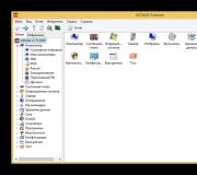
There are several ways to find out which driver you need to look for. First you need to get into “” and then into “”.
In most cases, problems are found in the "" section. If you click on this item, a drop-down list will open, on the left side of which there will be yellow exclamation mark, and then there is an inscription.

So, for example, you need to find a PCI controller driver Simple Communications. This means that there is no special interface found on the computer between the host and the firmware Management Engine from Intel.
Another popular problem is the presence of an error in Nvidia nforce PCI Management. It indicates a problem with the chipset software. To solve you need to go to official website and find the appropriate software. It is important to find exactly the right security (must match Windows versions, bit depth and even BIOS release). Then you can simply update the driver or install it if it was not there. Sometimes a reboot is required.

Search by ID( )
Sometimes there are situations when you cannot immediately determine which equipment is not working. Also, the marking in " Device Manager" What to do in this case?
To find what you need for Windows 7 software, you need to do a few movements:

By the way, this method is also suitable for PCI Windows XP devices. It is best to search on trusted sites to avoid accidentally installing a virus.
I have been asked this question more than once, so now I will try to answer it as clearly and briefly as possible, for this I will provide pictures of expansion slots PCI Express and PCI on the motherboard for a clearer understanding and, of course, I will indicate the main differences in characteristics, i.e. very soon you will find out what these interfaces are and what they look like.
So, first, let's briefly answer the question, what exactly is PCI Express and PCI?
What is PCI Express and PCI?
PCI is a computer parallel input/output bus for connecting peripheral devices to the computer motherboard. PCI is used to connect: video cards, sound cards, network cards, TV tuners and other devices. The PCI interface is obsolete, so find e.g. modern video card, which connects via PCI, probably won’t work.
PCI Express(PCIe or PCI-E) is a computer serial bus I/O for connecting peripheral devices to the computer motherboard. Those. in this case, bidirectional serial connection, which can have several lines (x1, x2, x4, x8, x12, x16 and x32), the more such lines, the higher the throughput of the PCI-E bus. The PCI Express interface is used to connect devices such as: video cards, sound cards, network cards, SSD drives and others.
There are several versions PCI-E interface This: 1.0, 2.0 and 3.0 (version 4.0 will be released soon). Designated this interface usually like this PCI-E 3.0 x16, which means PCI Express 3.0 version with 16 lanes.
If we talk about whether, for example, a video card that has a PCI-E 3.0 interface will work on a motherboard that only supports PCI-E 2.0 or 1.0, the developers say that everything will work, just of course keep in mind that the bandwidth will be limited possibilities motherboard. Therefore, in this case, overpay for a video card with more new version PCI Express I think is not worth it ( if only for the future, i.e. Are you planning to purchase a new motherboard with PCI-E 3.0?). Also, and vice versa, let’s say your motherboard supports version PCI Express 3.0, and your video card supports version 1.0, then this configuration should also work, but only with PCI-E 1.0 capabilities, i.e. There is no limitation here, since the video card in this case will work at the limit of its capabilities.
Differences between PCI Express and PCI
The main difference in characteristics is, of course, throughput; for PCI Express it is much higher, for example, PCI at 66 MHz has a throughput of 266 MB/sec, and PCI-E 3.0 (x16) 32 Gb/s.
Externally, the interfaces are also different, so connecting, for example, a PCI Express video card to a PCI expansion slot will not work. PCI Interfaces Express with different numbers of lines are also different, I will now show all this in the pictures.
PCI Express and PCI expansion slots on motherboards
PCI and AGP slots
PCI-E x1, PCI-E x16 and PCI slots


PCI Express interfaces on video cards


That's all I have for now!
Every PC user has at least once opened the device manager on their computer. It doesn’t matter whether it’s a regular desktop computer or a laptop, you can find a so-called PCI controller everywhere. What is it and why is it needed on a computer? Where to look for it and what to do with it?
What is a PCI controller?
PCI is a universal connection bus various devices. Usually they are located on the computer motherboard and with their help various additional fees. Holders desktop computer It will be easier to find PCI slots on your PC. When you remove the side cover of the case, you will see your PC's motherboard, and on it are several large white connectors. These connectors are called PCI buses. With their help, you can connect a video card to the motherboard, sound card, boards with additional connectors(USB or COM), network card etc.
The PCI controller itself is part of the motherboard and is responsible for normal work the tires themselves and the devices connected to them. PCI slots may have different versions and are intended for various types of boards. If you look closely at the PC motherboard, you will notice that the connector for connecting the video card is different from the others. This is done because video cards have more high speed exchange data with motherboard, and they also consume more electricity. On motherboards you can also find a small PCI connector, which is designed for network or various other cards that consume less power and do not require a wide data transfer channel.
Installing a PCI Device
Choosing additional device for your PC, find out what version of PCI slots is installed on your motherboard. Remember, different versions of these connectors differ in their shape, so a device for one version of the connector will not be physically compatible with another version of the connector found on the motherboard.
Finding out whether a device is compatible with your motherboard is quite simple:
- Download Everest, install and run it.
- In the left column, select "Devices" and select "PCI devices" there. The central window of the program will be divided in two; the top window will list all devices that are connected to PCI buses. By clicking on the device, in the lower window you can see information about the device and the bus itself to which it is connected. There you can also find out the PCI bus version.
- You can do it easier and find a description of your motherboard on the Internet, and then simply compare it with the characteristics of the device you want to install. You can find out the motherboard model using Everest programs, opening the "motherboard" section.
If the selected board is compatible with your motherboard, you can proceed to installing the device directly.
- Remove the side cover of the PC case.
- Select the PCI slot in which the device will be installed, or remove the device you want to replace with a new one from the desired slot.
- Just carefully insert the card so that it fits completely into the connector. You can't go wrong here, since it is physically impossible to install the board incorrectly into the connector.
- Connect additional connectors (if required) and replace the housing cover.
- Start your PC. When the OS boots you will see system message that a new device has been connected. Install the drivers necessary for its operation from installation disk, which comes with the device, by downloading the driver from the network or using automatic installation drivers.
Problems arising with the PCI controller
Sometimes after reinstalling the OS you may experience next problem- the system will not be able to recognize the PCI controller. When you open Device Manager, you will find the item “unknown hardware” instead of “PCI controller”. The solution to the problem is very simple - download required driver from your motherboard manufacturer's website and install it.
Hello. We would like to tell you how to solve the problem when installing the driver. PCI controller A.
Recently they brought to us Asus laptop, after installing the driver
It turned out that the driver does not work correctly.
It was necessary to install an operating room Windows system 7. After installing the operating system, all drivers were installed sequentially, as expected with a reboot. The drivers were installed from the official Asus website.
This problem has come to light. Device driver Trusted Execution Engine Interface does not work correctly. Updating the driver did not produce any results, everything remained unchanged.
It was decided to remove the drivers for this device completely. After uninstalling and rebooting, the system showed that there are no drivers for - PCI encryption/decryption controller.
Briefly PCI controller — This universal tire to connect various devices, we began to look for a solution to the problem in this direction.
How to solve this problem:
The first option to solve this problem is to set it in the BIOS settings to Advanced section OS Selection parameter, the operating system you are installing, in our case windows 7. If this option is not available, then you need to update the BIOS.
Then there in BIOS function Set Boot Option UEFI to Disabled and disable it. Now install the operating system from your DVD media or USB doesn't matter.
After installing the operating system, install drivers other than the Intel(R) driver Trusted Execution Engine Interface.
Then install the update for Windows 7 - Kernel-Mode Driver Framework version 1.11 update for Windows 7, this update is still named KB2685811 in the update center.
You can download it from the official Microsoft website
or we have a Yandex disk, version for x64, version for x86.
Then install drivers for Intel(R) Trusted Execution Engine Interface or PCI encryption/decryption device.
As we did.
In our case, the operating system was not reinstalled and no changes were even made to the BIOS; we simply removed the drivers for this device, then downloaded and installed the update mentioned above. We didn’t do anything anymore; the drivers were detected by the system and installed automatically. Just rebooted the laptop after the update was completed.